show advanced search
-
1-6 / 6
- display number
-
order by date
-
order by researcher's name
-
order by affiliation

2916
Nanotechnology / Materials
posted:2025/10/20
表面増強ラマン散乱分光用光学素子及び表面増強ラマン散乱分光装置
HOMMA, Takayuki Professor (Faculty of Science and Engineering School of Advanced Science and Engineering)

2699
Nanotechnology / Materials
posted:2025/07/08
特開2025-039048
銀触媒核を用いた高機能アニオン交換膜の無電解析出プロセス
HOMMA, Takayuki Professor (Faculty of Science and Engineering School of Advanced Science and Engineering)
本発明はアニオン交換膜上に安価な銀を触媒核として用い、広範な金属または合金薄膜を無電解析出により形成する新たな製造方法です。従来のパラジウムに比べて高性能・低コストな代替技術を実現します。
2024-0206-02
Nanotechnology / Materials
posted:2024/02/06
The New Interface Measuring Device using New Plasmon Sensor and Raman Scattering Spectroscopy
HOMMA, Takayuki Professor (Faculty of Science and Engineering School of Advanced Science and Engineering)

2016-0203-05
Nanotechnology / Materials
posted:2016/02/03
The new interface measuring device using new plasmon sensor and raman scattering spectroscopy
HOMMA, Takayuki Professor (Faculty of Science and Engineering School of Advanced Science and Engineering)
● Molecular configuration at buried interface, i.e. solid / liquid, Chemical structure change of the atomic level, are simply measured in nanometer scale.
2015-0303-04
Nanotechnology / Materials
posted:2015/03/03
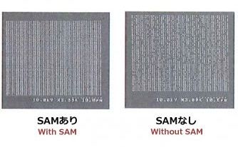
Electroforming Technique using Self-assembled Monolayer(SAM) for Modified Nanopatterns
HOMMA, Takayuki Professor (Faculty of Science and Engineering School of Advanced Science and Engineering)
collaborative researchers:SAITO, Mikiko Senior Researcher
・Electroless NiP nanoimprinting mold replicated from Self-assembled Monolayer (SAM) modified Nanopatterns ・Elaborately manufactured in nano size and complicated form
2014-0122-02
Nanotechnology / Materials
posted:2014/01/23
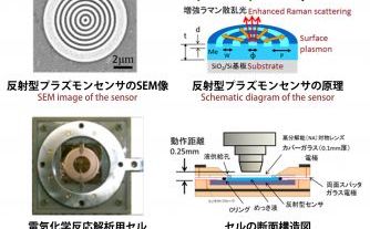
新規なプラズモンセンサ及びラマン分光法を用いた界面計測技術
HOMMA, Takayuki Professor (Faculty of Science and Engineering School of Advanced Science and Engineering)
・表面プラズモンセンサと表面増強ラマン散乱を応用したラマン分光法による界面計測技術・新規なナノ構造の「反射型プラズモンセンサ」を開発・測定物に対応した自由なセンサ部の設計が可能・固液界面を深さ分解能0.1nm以下、非破壊での観察を実現