Electroforming Technique using Self-assembled Monolayer(SAM) for Modified Nanopatterns
2015-0303-04


- researcher's name
- affiliation
- research field
-
Nano/Microsystems,Functional solid state chemistry,Electron device/Electronic equipment
- keyword
-
predominance
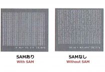
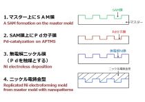
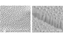
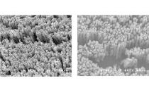
・Electroless NiP nanoimprinting mold replicated from Self-assembled Monolayer (SAM) modified Nanopatterns
・Elaborately manufactured in nano size and complicated form
background
・Additional value and functionalization of products
・Super-high aspect ratio&Nano-fabrication achievement
・It is hard process by the conventional electroless plating or sputtering process
summary
・Pretreatment process by SAM
・The metallic molds with super-high aspect ratio can be manufactured easily
application/development
・Provide Ni electroforming mold with super-high aspect ratio (LEAP Co.,Ltd)
material
collaborative researchers
SAITO, Mikiko Senior Researcher (Research Council (Research Organization) Institute for Nanoscience & Nanotechnology) (retired)
related paper
- C. P. Lin, M. Saito, and T. Homma, “Fabrication of elctroless NiP nanoimprinting mold by replication of UV-treated and self-assembled-monolayer-modified cyclo-olefin polymer nanopatterns ”, Electrochemistry, Vol. 81 (2013) pp. 678-681
- C. P. Lin, M. Saito, and T. Homma, “Nanoindentation analysis for mechanical properties of electroless NiP imprinting moldreplicated from self-assembled-monolayer modified master mold”, Jpn. J. Appl. Phys., Vol. 52, (2013)
- C. P. Lin, M. Saito, and T. Homma, “Initial Catalyzation Analysis of Electroless NiP Nanoimprinting Mold Replicated from Self-assembled Monolayer Modified Nanopatterns”, Electrochimica Acta, Vol. 82, (2012) pp. 75 -81.
same researcher's seeds

posted:
2015/03/03