The new interface measuring device using new plasmon sensor and raman scattering spectroscopy
2016-0203-05


- researcher's name
- affiliation
- research field
-
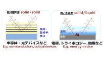
Nano/Microsystems,Functional solid state chemistry,Electron device/Electronic equipment
- keyword
-
background
● Non-destructive depth profile analysis, is difficult
● High-precision nondestructive inspection is difficult
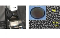
● Complicated operations of large measurement equipment.
● High-precision nondestructive inspection is difficult
● Complicated operations of large measurement equipment.
summary
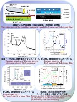
● Molecular configuration at buried interface, i.e. solid / liquid, Chemical structure change of the atomic level, are simply measured in nanometer scale.
predominance
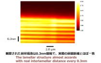
● Depth-resolution 0.1nm or less (More than 10 times of the present sensitivity)
● High-precision nondestructive inspection,low cost and high measurement convenience
● High-precision nondestructive inspection,low cost and high measurement convenience
application/development
● High-density optical recording multilayer film, a variety of devices, i.e. magnetic disks or semiconductors, Li ion battery, fuel cell, vital reaction, and so on.
material
same researcher's seeds

posted:
2016/02/03