show advanced search
-
1-10 / 10
- display number
-
order by date
-
order by researcher's name
-
order by affiliation
2023-0127-01
Nanotechnology / Materials
posted:2023/01/27
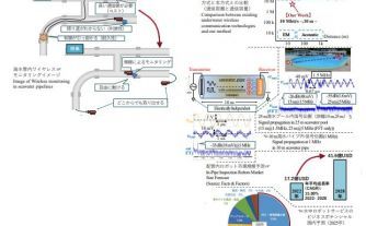
海水のイオン導電性を利用した海中無線通信 ~海水管,漁業用いけす内のワイヤレスリアルタイムモニタリングが可能に~
KAWARADA, Hiroshi Professor (Faculty of Science and Engineering School of Fundamental Science and Engineering) (retired)
collaborative researchers: 佐藤 弘隆 (retired), 正留 康太 (retired), 野本 玲於奈 (retired)

2316
Nanotechnology / Materials
posted:2020/11/12
特許第7491547号
ダイヤモンド電界効果トランジスタ及びその製造方法
KAWARADA, Hiroshi Professor (Faculty of Science and Engineering School of Fundamental Science and Engineering) (retired)
2020-0131-03
Nanotechnology / Materials
posted:2020/02/06
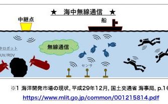
Development of new electric wireless seawater communication
KAWARADA, Hiroshi Professor (Faculty of Science and Engineering School of Fundamental Science and Engineering) (retired)
● Electric communication utilizing conductivity of seawater● Transmitter : metal electrode ⇔ Receiver : transistor shape sensor operating in solutions● Apply square wave voltage to metal electrode &nb...
2039
Nanotechnology / Materials
posted:2018/04/18
 第7017016号
ノーマリオフ動作ダイヤモンド電力素子及びこれを用いたインバータ
KAWARADA, Hiroshi Professor (Faculty of Science and Engineering School of Fundamental Science and Engineering) (retired)
1843
Nanotechnology / Materials
posted:2017/03/06
特許第6205017号
トランジスタの製造方法及びセンサ素子
KAWARADA, Hiroshi Professor (Faculty of Science and Engineering School of Fundamental Science and Engineering) (retired)
2016-0203-08
Nanotechnology / Materials
posted:2016/02/03
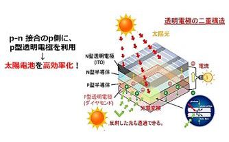
Boron-doped nanocrystalline diamond as a p-type transparent electrode
KAWARADA, Hiroshi Professor (Faculty of Science and Engineering School of Fundamental Science and Engineering) (retired)
collaborative researchers:古閑 三靖 (retired)
● Production method of the p-type conduction of high Boron-doped NCD with high transmittance and excellent electrical characteristic● Achieving two layers which High Boron-doped NCD was grown on top of undoped transparent NCD with quartz substrate
2016-0203-07
Nanotechnology / Materials
posted:2016/02/03
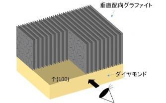
Vertically oriented graphite layers on diamond substrate
KAWARADA, Hiroshi Professor (Faculty of Science and Engineering School of Fundamental Science and Engineering) (retired)
collaborative researchers:INABA, Masafumi Part-time Lecturer (retired)
● Implant ions to diamond (100) surface at high temperature ● Interstitial carbon atoms defuse to the diamond surface during the thermal treatment (1700oC, 2h) after implantation● High density vertically oriented graphite layer was formed on diamond surface
2016-0203-06
Nanotechnology / Materials
posted:2016/02/03
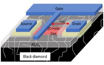
MOSFET on polycrystalline diamond
KAWARADA, Hiroshi Professor (Faculty of Science and Engineering School of Fundamental Science and Engineering) (retired)
collaborative researchers:モフド シャムスル ナシリク ビン サムソル バハリン (retired), INABA, Masafumi Part-time Lecturer (retired), 北林 祐哉 (retired), 柴田 将暢 (retired)
● We developed high breakdown voltage MOSFET with polycrystalline black diamond ● The device exhibits perfect modulation and good device characteristic pinch off and saturation region● High voltage breakdown of 1824 V by black polycrystalline diamond
2014-0122-05
Nanotechnology / Materials
posted:2014/01/23
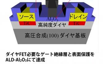
ダイヤモンド半導体を用いた高信頼性電力素子
KAWARADA, Hiroshi Professor (Faculty of Science and Engineering School of Fundamental Science and Engineering) (retired)
・550℃の大気中でも導電性が確保され、絶縁性が向上した保護膜の製造方法・表面を水素化したダイヤモンド基板上に2層の保護膜を形成することで実現