New Wide Bandgap Semiconductor --- β-Ga2O3 Single Crystal
2015-0303-03


- researcher's name
- affiliation
-
- keyword
-
predominance
・The proposal and actual proof of β-Ga2O3 single crystal as a new wide bandgap semiconductor
・Advantageous growth nature of β-Ga2O3 single crystals from melt under atmospheric pressure.
・Wide controllability of conductivity (Large band gap energy (4.8~4.9V)
background
・Expectation for the new material beyond GaN, SiC semiconductors
summary
・Realization of the large-sized single crystal from melt by EFG method
・Conductivity control -Development of the n-type, insulating and p-type dopants
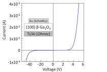
・Development of ohmic and schottky electrodes
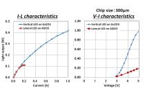
・The proposal and actual proof as substrates for LED
application/development
・Available now by Tamura Corporation
・Substrates for power devices and Visible/UV LEDs
・Diverse applications, such as high brightness LEDs, UV sensors, and etc
material
collaborative researchers
SHIMAMURA, Kiyoshi Guest Professor , ガルシア ビジョラ (独立行政法人 物質・材料研究機構)
posted:
2015/03/03