show advanced search
-
1-5 / 5
- display number
-
order by date
-
order by researcher's name
-
order by affiliation

2039
Nanotechnology / Materials
posted:2018/04/18
 第7017016号
ノーマリオフ動作ダイヤモンド電力素子及びこれを用いたインバータ
KAWARADA, Hiroshi Professor (Faculty of Science and Engineering School of Fundamental Science and Engineering)
2016-0203-07
Nanotechnology / Materials
posted:2016/02/03
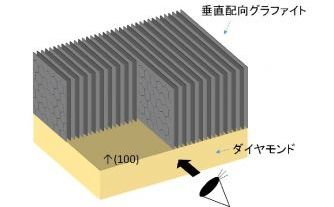
Vertically oriented graphite layers on diamond substrate
KAWARADA, Hiroshi Professor (Faculty of Science and Engineering School of Fundamental Science and Engineering)
collaborative researchers:INABA, Masafumi Part-time Lecturer
● Implant ions to diamond (100) surface at high temperature ● Interstitial carbon atoms defuse to the diamond surface during the thermal treatment (1700oC, 2h) after implantation● High density vertically oriented graphite layer was formed on diamond surface
2016-0203-06
Nanotechnology / Materials
posted:2016/02/03
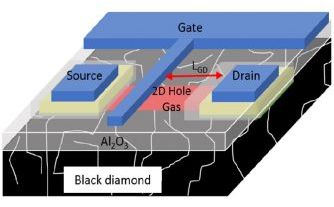
MOSFET on polycrystalline diamond
KAWARADA, Hiroshi Professor (Faculty of Science and Engineering School of Fundamental Science and Engineering)
collaborative researchers:モフド シャムスル ナシリク ビン サムソル バハリン , INABA, Masafumi Part-time Lecturer , 北林 祐哉 , 柴田 将暢
● We developed high breakdown voltage MOSFET with polycrystalline black diamond ● The device exhibits perfect modulation and good device characteristic pinch off and saturation region● High voltage breakdown of 1824 V by black polycrystalline diamond

1736
Manufacturing Technology
posted:2015/11/03
2017-45897
多結晶ダイヤモンド上のパワーMOSFET(ダイヤモンド電界効果トランジスタ及びその製造方法)
KAWARADA, Hiroshi Professor (Faculty of Science and Engineering School of Fundamental Science and Engineering)
◆多結晶ダイヤモンド(黒い)上にMOSFETを作製 ◆顕著な変調・良好なデバイス特性◆逆阻止耐圧1800Vを達成