Boron-doped nanocrystalline diamond as a p-type transparent electrode
2016-0203-08

- researcher's name
-
about researcher KAWARADA, Hiroshi Professor (retired)
- affiliation
-
Faculty of Science and Engineering School of Fundamental Science and Engineering
- research field
-
Electronic materials/Electric materials
- keyword
-
background
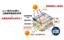
● For the high efficiency of the device, the p-type transparent electrode is necessary, but difficult to product stably
● ITO as the transparent electrode is the n-type semiconductor
● Indium(In) of ITO has the problem-the issue of resources, a price remarkable rise and the steady supply
summary
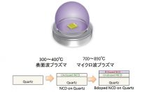
● Production method of the p-type conduction of high Boron-doped NCD with high transmittance and excellent electrical characteristic
● Achieving two layers which High Boron-doped NCD was grown on top of undoped transparent NCD with quartz substrate
● Achieving two layers which High Boron-doped NCD was grown on top of undoped transparent NCD with quartz substrate
predominance
● Achieved more than 90% of transmittance, and less than seat resistance 300Ω/sq by the p-type conduction of high Boron-doped nanocrystalline diamonds(NCD) simultaneously
● High hole mobility values 2 to 4 cm2V-1s-1
● ITO alternatives for transparent conductors
● High hole mobility values 2 to 4 cm2V-1s-1
● ITO alternatives for transparent conductors
application/development
● Flat panel display such as liquid crystal panel, plasma display panel, organic electroluminescence display
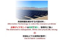
● Solar cell’s devices including for the usage in harsh conditions
● Solar cell’s devices including for the usage in harsh conditions
material
collaborative researchers
古閑 三靖 (理工学術院 先進理工学研究科)
same researcher's seeds
-
 MOSFET on polycrystalline diamond
 -
 Vertically oriented graphite layers on diamond substrate
 -
 Development of new electric wireless seawater communication
posted:
2016/02/03


