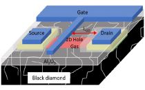
MOSFET on polycrystalline diamond
2016-0203-06

- researcher's name
-
about researcher KAWARADA, Hiroshi Professor (retired)
- affiliation
-
Faculty of Science and Engineering School of Fundamental Science and Engineering
- research field
-
Electronic materials/Electric materials
- keyword
-
background
● Large wafers are necessary for power device materials
● Diamond is one of the promising power semiconductor material
● Polycrystalline diamond is suitable to enlarge wafer
● Diamond is one of the promising power semiconductor material
● Polycrystalline diamond is suitable to enlarge wafer
summary
● We developed high breakdown voltage MOSFET with polycrystalline black diamond
● The device exhibits perfect modulation and good device characteristic pinch off and saturation region
● High voltage breakdown of 1824 V by black polycrystalline diamond
● The device exhibits perfect modulation and good device characteristic pinch off and saturation region
● High voltage breakdown of 1824 V by black polycrystalline diamond
predominance
● High powered
● Low cost
● Manufacturing possibility
● Low cost
● Manufacturing possibility
application/development
● High-voltage, direct current (HVDC)
● Electric vehicles
● Automaton
● Etc.
● Electric vehicles
● Automaton
● Etc.
material

collaborative researchers
モフド シャムスル ナシリク ビン サムソル バハリン (理工学術院 電子物理システム学科) , INABA, Masafumi Part-time Lecturer (retired) , 北林 祐哉 (理工学術院 電子物理システム学科) , 柴田 将暢 (理工学術院 電子物理システム学科)
same researcher's seeds
-
 Vertically oriented graphite layers on diamond substrate
 -
Boron-doped nanocrystalline diamond as a p-type transparent electrode
-
Development of new electric wireless seawater communication
posted:
2016/02/03